
I am currently putting the finishing touches on another printed circuit board.
A PCB is laid out with specialized software, drawn on the computer screen. The software can then generate CAM files that are sent to a board house, a manufacturer who can take these files and create a physical PCB. The PCB is thin layers of copper etched to create the patterns of traces laminated onto a fiberglass substrate. When designing the PCB each component, each copper conductor, each trace, is carefully positioned by the designer on the screen, dragging objects colored lines about to create a solution.
Unlike more formal puzzles the rules for solving a PCB is very free-form. While there is no right answer, there are better answers, cleaner solutions. A good PCB design will work well, a bad one may not work at all. Bad designs happen, even to careful designers.
A good PCB will create a working electrical circuit that has to obey the laws of physics. In this world impedance is everything. Impedance is the sum of a circuit’s resistance, inductance and capacitance. The width, length, and shape of a copper trace will determine its impedance.
Just running a copper trace from one point to another to make each connection is not enough. Some traces will carry more current, some might have high speed digital switching signals on them, others might carry sensitive analog signals. The rules for each trace changes on the nature of the signal. Some traces can follow roundabout paths without problems, others must be short to avoid radiating noise, or wide to carry more current. Some traces may not be located near other traces. The designer must keep all of these factors in mind while drawing each trace.
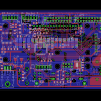
Tying everything together is usually a ground plane, the reference against which all voltages are measured, to which all currents must return. Most boards include some sort of ground plane, a layer of copper as complete as possible to serve as this low impedance reference.
To create a good solution in only two layers, front and back, can increase the challenge dramatically. Double layer PCB’s are cheap and very common, but harder to design a good circuit on. Single layer are even cheaper, but only simpler circuits can be successfully produced.
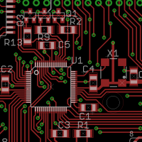
This latest PCB of mine is to be a double-layer, plated-through-hole design, very standard technology. To accomplish this I have positioned most of the components and traces on one side, leaving the other side available for ground plane. There are interruptions of this plane, areas where other traces are run, but the plane seems to be relatively intact.
A completed PCB is a work of art, an expression of skill, the summation of a thousand lessons learned across a career in electronics. Of course I will not know just how good a solution to this puzzle I have found until I really build a circuit on it. I will have to solder up a real PCB and test a real circuit. It may look good on the screen, but despite the care I take in layout there may be a small mistake or two.

show us your solder skills young Andrew
aloha
Just a TQFP package with 0.5mm leads, not that much of a challenge.