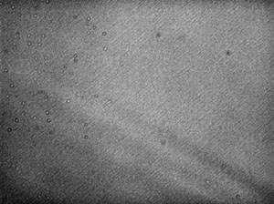
The manufacturing processes that create CCD's are seldom perfect. Often there are slight variations across the surface of the chip that results in slight sensitivity differences. These effects can be caused by variations in the base silicon, variations in the masks that create the layers or the chemical processes used to create the layers. These differences result in minor variations in the sensitivity of each pixel that can be seen in a flat field. There is no real problem with these differences, the pattern is consistant and can be corrected with proper application of a flat field. Just another reason to do proper image calibration.
The examples shown here are quite subtle until the image is dramatically stretched. These effects will often go unnoticed in normal images, but may become important when processing the low level parts of astronomical images such as fine nebula detail or the outer edges of a galaxy.
Back-thinned chips are particularly subject to several effects that can affect photoresponse uniformity. These can result from the mechanical or chemical thinning process or variations in the AR coating, note the patterns shown by the E2V CCD87 to the right.