
When you want to see the stars, find someplace dark

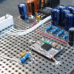
I have had hardware for a while now, it is about time I release some firmware that actually runs it.

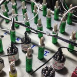
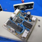
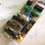
The first GenPIC code revision is a test and demonstration release. It contains support for one serial port, an LCD character display, user input including the encoder and pushbuttons, the indicator LED’s, timer generation, analog input including onboard temperature readout.
Also included is a serial command interpreter implementing a serial interface usable with any serial terminal. There is also a user interface system with a state setup that provides multiple input screens. This should handle a wide array of basic control capabilities, either using the serial port or through using the LCD screen and the encoder.
The code allows you to exercise many of the basic functions of the hardware and provide a framework on which a real application can be built.
It works, it runs, it looks fairly good. Now time to make something useful with it…
| First code release 11Feb2017 |
Code Rev0.1 |
There will be additional code releases as this project continues, as always check the GenPIC main post for the latest!
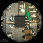
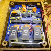
The rotary encoder is a popular input device for many microcontroller devices. A knob that can be used to increase or decrease a setting with a nice tactile click for each increment. You can even get an integral pushbutton, just rotate for the setting then press the same knob to enter. With some clever programming you can create a one device user interface using only the encoder.

I have integrated a rotary encoder in the GenPIC utility board. With the combination of an LCD display and the rotary encoder you have all the ingredients for a functional user interface arranged neatly for a panel mount unit.
In the past I have simply set an interrupt to fire on the edge of one channel, then sampled the opposite channel to detect the direction. With the addition of a small delay to debounce the result. This worked well in previous devices, but this time I encountered trouble, the direction sampling was erratic, the value going up when it should have gone down and vice-versa.
Breaking out my logic analyser I found out why, this particular encoder proved to be somewhat noisier than I had seen in the past, with notable periods of bouncing signals.
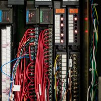
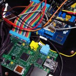
Over the years I have hand wired so many microcontroller PCB’s. Along with my own projects for myself there are more than a dozen of my little microcontroller devices at work about the observatory. The OSIRIS IR calibration source, the Keck 2 dome inclinometers, a precipitation sensor interface, the Keck 1 AO electronic vault temperature sensors, the weather mast fan and shelter controller, the list goes on. Anyplace a bit of electronic intelligence is needed for the task.
While a couple of my microcontroller designs have been laid out on proper circuit cards, like the SciMeasure camera exposure controllers, I have never laid out a general purpose microcontroller PCB. This is not for lack of thinking about it, so many times I have considered this could be so much easier if I could only invest a little time in a layout.
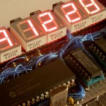
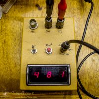
I have been messing about with electronic circuitry for almost four decades. I recently came across an early example of my work. The device is a digital event counter built around classic 74xx series logic. A chain of 74190 decade counters feed a set of 7447 decoder drivers and seven segment LED displays. A plastic project case with switches and connectors reminds me I have been building little devices for a very long time.
I am preparing to release a design under the Open Source Hardware Association definition. By releasing a design this way you allow the electronic maker community to freely share and use the design. When following the community rules for open hardware, you can mark your equipment with the open source hardware logo. The logo itself is released under a Creative Commons licence (CC-SA) and is likewise free to copy and use, if you follow the rules.
While the OSHWA website links the logo in KiCAD and several other formats, it does not provide the logo in Eagle format. Off to the web to find an Eagle library with the logo… Hmmm… Found one, but it has issues.
![]()
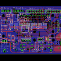
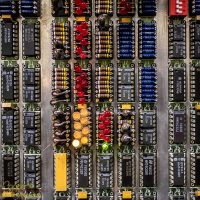
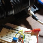
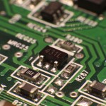
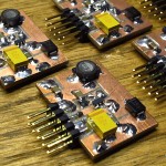
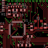
I am currently putting the finishing touches on another printed circuit board.
A PCB is laid out with specialized software, drawn on the computer screen. The software can then generate CAM files that are sent to a board house, a manufacturer who can take these files and create a physical PCB. The PCB is thin layers of copper etched to create the patterns of traces laminated onto a fiberglass substrate. When designing the PCB each component, each copper conductor, each trace, is carefully positioned by the designer on the screen, dragging objects colored lines about to create a solution.
The golden yellow glow that has dominated the night for generations is disappearing.

The yellow glow of sodium light has been both celebrated and reviled. While the glow can be attractive in night scenery it also creates inhuman tones in faces and photos of people. Movies have been shot under sodium lights, songs reference the golden glow. Astronomers both professional and amateur prefer the lights as the light can be easily filtered from view.
It is always a good day when I drive up the mountain to a broken telescope, then drive down leaving a working telescope. Easy to say, not always easy to accomplish, the simple statement obscuring a day of struggle to solve the problem and fix it.

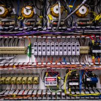
The Keck 2 telescope drive is a complex beast of dozens of relays, miles of cabling, servo amplifiers and power supplies, plus several circuit boards designed and built in the 1980’s holding a bewildering array of arcane logic.
The Keck Adaptive Optics systems are workhorse scientific instruments. Equipment that has resulted in so many great astronomical discoveries. The AO systems have also seen a great deal of improvements and upgrades through the years. New computers, a new wave-front controller, guide star lasers added, new cameras, different science instruments, and much more.

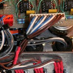
Eventually I just get fed up with it and insist we spend some time getting rid of it. With no AO use scheduled for a while there is a chance to spend a couple days ripping out this pile of cruft. Identifying and removing unused boxes. Following cables to nowhere, wire cutters in hand to snip away the multitude of nylon zip-ties.
We remove three large armloads of cables and other gear, carring the pile down to the electronics lab for sorting through and disposal. Most of it is horribly obsolete, things like KVM’s for PS/2 style mice and keyboards, or cables for old Sun computers. Most of it will simply be thrown out. It feels so good to get it out of AO and to clean up the place a little.
I called this pile of junk cruft, a word that drew funny looks from my co-workers. You don’t know what cruft is? What sort of nerds are you? Sorry, cruft is what I have always called leftover technical junk.
Cruft is jargon for anything that is left over, redundant and getting in the way. It is used particularly for superseded and unused technical and electronic hardware and useless, superfluous or dysfunctional elements in computer software. – Wikipedia
It turns out that the word has a long history in engineering and computer science with a heritage that includes MIT and Harvard. It is indeed the proper word for the detritus that had been accumulating in the AO vault.