
I am currently putting the finishing touches on another printed circuit board.
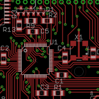
A PCB is laid out with specialized software, drawn on the computer screen. The software can then generate CAM files that are sent to a board house, a manufacturer who can take these files and create a physical PCB. The PCB is thin layers of copper etched to create the patterns of traces laminated onto a fiberglass substrate. When designing the PCB each component, each copper conductor, each trace, is carefully positioned by the designer on the screen, dragging objects colored lines about to create a solution.