Some equipment around the observatory is thirty or more years old. As you would expect, keeping it running can be a challenge.
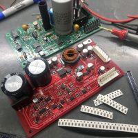
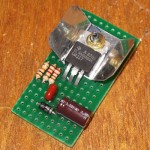
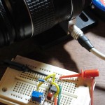
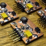
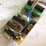
A redesigned small signal PCB for an Inland Motor FCU-100-30 amplifier power supply
There are two ways of dealing with this old equipment… Replacing it with something new is the preferred way. When it becomes difficult to locate spare parts, when it breaks down too often, just replace it with new gear. For much of the equipment this is the usual answer and is often a major part of the job.
Some equipment is not so easily replaced. When replacement would require wholesale redesign of a system it becomes more of a challenge. Sometimes the only choice is to keep that old gear running.
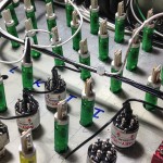
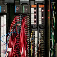
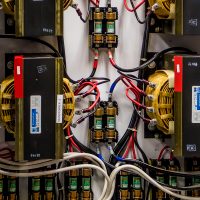
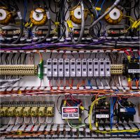
This is the case with our servo amplifiers. Twelve amplifiers supply the power that drives the telescope, one amplifier for each motor. Eight amplifiers and motors drive azimuth, four drive elevation. Three hundred and seventy tons moved by twelve relatively small DC motors. While much of the telescope control system was recently replaced, it was decided to keep the old servo amplifiers.
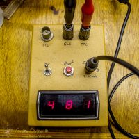
You might notice that these servo amplifiers are just a wee bit critical.
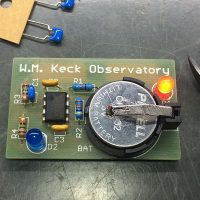
With the Keck Observatory open house approaching I am helping get one of the most popular activities ready. At the last two open houses we have made flasher pins, we will do so again this year.
A simple electronics project… The Flasher PinFlashers? These are a simple circuit built on a PCB that flashes a pair of LED’s. Nothing serious, just a bit of electronics fun. The activity allows folks to learn a little electronics and soldering.
The PCB is configured as a pin or badge, with a brooch pin soldered to the back that also serves as a switch to turn on the LED’s.
The original design came from John Maute at SAO. The circuit is based around the venerable LM555 timer IC configured as an astable multivibrator. The LM555 timing circuit is simple enough to solder together in a few minutes, complex enough to look cool and provide a real introduction to an electronic circuit.
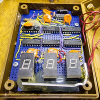
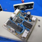
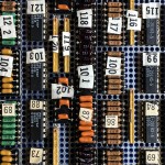
Over the years I have hand wired so many microcontroller PCB’s. Along with my own projects for myself there are more than a dozen of my little microcontroller devices at work about the observatory. The OSIRIS IR calibration source, the Keck 2 dome inclinometers, a precipitation sensor interface, the Keck 1 AO electronic vault temperature sensors, the weather mast fan and shelter controller, the list goes on. Anyplace a bit of electronic intelligence is needed for the task.
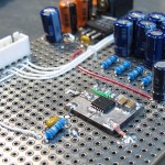
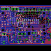
A PCB assembly in layoutOf course the challenge is that each of these controllers has been hand wired and built for a specific task. This takes a few hours of running little wires on a perfboard. And while I enjoy such wiring, it does make the task take notably longer.
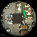
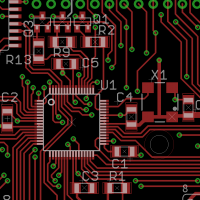
While a couple of my microcontroller designs have been laid out on proper circuit cards, like the SciMeasure camera exposure controllers, I have never laid out a general purpose microcontroller PCB. This is not for lack of thinking about it, so many times I have considered this could be so much easier if I could only invest a little time in a layout.
I am currently putting the finishing touches on another printed circuit board.
A PCB assembly in layoutLayout of a printed circuit board, or PCB, is one of the most complex puzzles I know. Creating a complex PCB takes a great deal of knowledge, a lot of patience, and a robust set of puzzle solving skills. These are the same sort of puzzle skills that might be used to solve a Sudoku or a tough crossword puzzle. Seeing patterns, spotting errors, trial and error, planning ahead, all skills used to their utmost in laying out a PCB.
A PCB is laid out with specialized software, drawn on the computer screen. The software can then generate CAM files that are sent to a board house, a manufacturer who can take these files and create a physical PCB. The PCB is thin layers of copper etched to create the patterns of traces laminated onto a fiberglass substrate. When designing the PCB each component, each copper conductor, each trace, is carefully positioned by the designer on the screen, dragging objects colored lines about to create a solution.
I am no stranger to point-to-pointwiring. I routinely use the technique to build small circuit boards. Well done point-to-point is a permanent and reliable way to build a complex electronic device.
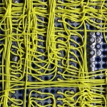
Welded point-to-point wiring on a complex circuit board
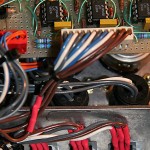
But then there is this circuit board assembly I came across… At first glance it looks like a wire wrap board. But there are no posts, the wires are flush to the board. Neither is it traditional point-to-point wiring, the wires are not terminated to solder pads beside the pins being connected. I had never seen a construction technique like this.
The board is an old PCB assembly found in a storage cabinet while clearing out the old junk that has accumulated about the observatory. No idea where it came from or what it was used for, the only clue is some writing on the box… “Keck level shifter”, Perhaps a piece of a detector controller? Someone clearly put a lot of work into the board at one time, now it sits in my office as unknown junk. It is the odd construction technique that caught my eye and led me to hang on to the board, at least temporarily. What is this?
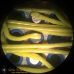
A closer look under a microscope shows a connection clearly made by some sort of spot welder. There is a neat little hole through the insulation at each connection. Stripping back the insulation reveals a very neatly welded wire. Each wire is welded to the flat bottom of each pin socket. Every component pin is socketed, this includes all passives, which are mounted to headers and plugged in alongside the IC’s.
There are a number of advantages to this wiring method… The connections should be very reliable and robust, the weld is a nearly ideal electrical connection. As no connection pads are needed beside each socket the density is much higher using less circuit board real estate per component, you can cram more on the board. Interestingly the connection technique can be used without terminating the wire, daisy chaining to the next connection point.
There are disadvantages as well… The method clearly requires some sort of welding equipment with perhaps an automatic wire feeder and cutter, a built-in microscope for positioning the weld, and more. Clearly an expensive piece of kit. No components can be present during welding as they may suffer damage from the high electrical currents needed for spot welding, thus everything must be socketed. All those little sockets are expensive! Rework or repair would need to be done with more traditional soldering techniques.
I would love to see the machine that did this board assembly. Maybe even a chance to use it. More information on the process seems difficult to find on the web without a trade name or other keyword that would clearly identify the process.
Not that these welded wires would be of much use today. The technique is clearly ideal for complex digital circuits of the style and speed that was common through the 1980’s to around 2000 or so. After that the prevalence of surface mount technology and the abandonment of the DIP package would doom the method. Modern high speed circuits benefit greatly from the more controlled traces of a printed circuit board and would not fare well on a welded wire board. In these days of easy computer layout and cheap printed circuit boards welding would not be my fabrication method of choice.
Welded point-to-point wiring on a complex circuit board
Detail of a connection in welded point-to-point wiring on a complex circuit board
Detail of a weld in welded point-to-point wiring on a complex circuit board
Component side of a welded point-to-point circuit asembly